If you need to transcode an 8K video in real-time, you're going to struggle to find hardware capable of keeping up. We've found that not even the beefiest of GPUs can decode a high bitrate 8K stream in real-time (not to mention re-encode it). To transcode such a beastly stream, you can scale horizontally and send segments to workers in a cluster. This gets you real-time, but comes with a heavy price in terms of cost and latency. So how is it that hardware manufacturers like Blackmagic Design are able to encode 12K streams in real-time on small devices like handheld cameras?
The Secret
The secret is in FPGAs.
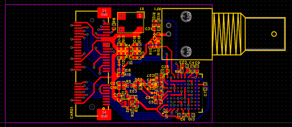
FPGAs can provide extreme hardware acceleration to fields like video processing and machine learning. Blackmagic Design, for example, is known to utilize Xilinx FPGAs during their development process. In the above image, taken directly from their website, you can see a Xilinx Spartan-6 FPGA powering their camera control shield.
You might wonder "If FPGAs are so powerful, why isn't everyone sticking them in their PCI-e slots instead of GPUs?" Well, some people actually are. Apple's relatively new Afterburner Card is effectively that: It uses an FPGA to accelerate their ProRes codec.
Programming an FPGA
A simple mental model for FPGAs is to think of them as arrays of NAND gates. NAND gates are "universal" in the sense that you can create all other logic gates using NAND gates alone, and a sufficiently large array of NAND gates can be connected to make anything.
Traditionally, programming those connections is done in a hardware description language (HDL) like Verilog or VHDL. Today, there are several higher level alternatives available. For example, a common technique is to synthesize C or C++ into an HDL.
For this blog post, we're going to program an FPGA, but we're going to go even higher level. We're going to use Xilinx Vivado to simply drag and drop things into place.
The goal will be to use an FPGA to scale unencoded video, supporting inputs and outputs of any resolution up to 8K.
The FPGA Image
Amazon has a class of EC2 instances named "F1" that have a Xilinx UltraScale Plus FPGA attached via PCI-e. These are readily available to anyone with an AWS account, so we're going to use one.
The following is a gentle introduction to the workflow and concepts required to implement an FPGA solution. It doesn't come with project files or complete code, but combined with the thorough documentation in the aws/aws-fpga repository, any software engineer should be able to reproduce these results within a day or two of reading and experimenting.
After creating a new IPI project in Vivado, you'll find yourself with an IP block representing your connection to the EC2 instance:
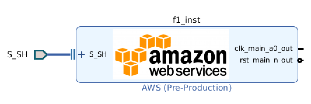
This block has three things by default:
- S_SH: This is the connection to the "shell", which connects you to the AWS platform and EC2 instance itself. This never changes.
- clk_main_a0_out: This is the default clock. You can change the clock speed or add more clocks. In our case, everything will use a single clock at the default speed of 125MHz.
- rst_main_n_out: This is the reset signal, which should reinitialize the entire FPGA to a fresh state.
Functionality is added by dropping IP blocks onto the block diagram. We want to scale video, and Xilinx happens to provide a free "multi-scaler" block just for that:
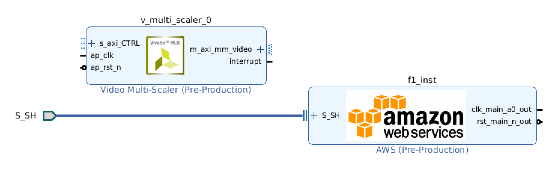
To understand how to connect this block, we need to two things:
- The documentation.
- A high level understanding of AXI4 (coming next).
The FPGA is attached to the EC2 instance via a PCI-e slot. Within this slot, there 6 "BAR"s that can be used to transfer data:
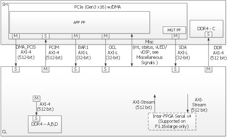
The protocol by which we transfer data across these BARs is AXI4. Furthermore, if we want to use the DDR4 memory available to the FPGA, we'll also be using AXI4 for that.
We don't need to know the specifics of the protocol, but the important part here is that there is always a controller ("M" in the diagrams), which issues read/write requests, and a device ("S") which fulfills them.
The multi-scaler block is memory-based, which means we'll write input frames to memory that it can access, send it a signal, then read the result from that same memory.
One way of doing that would be to connect it to the shell's PCIM BAR. By doing that, the multi-scaler would be able to read and write the EC2 instance's memory directly via DMA. A much simpler way, however, is to simply use the FPGA's DDR4 memory:
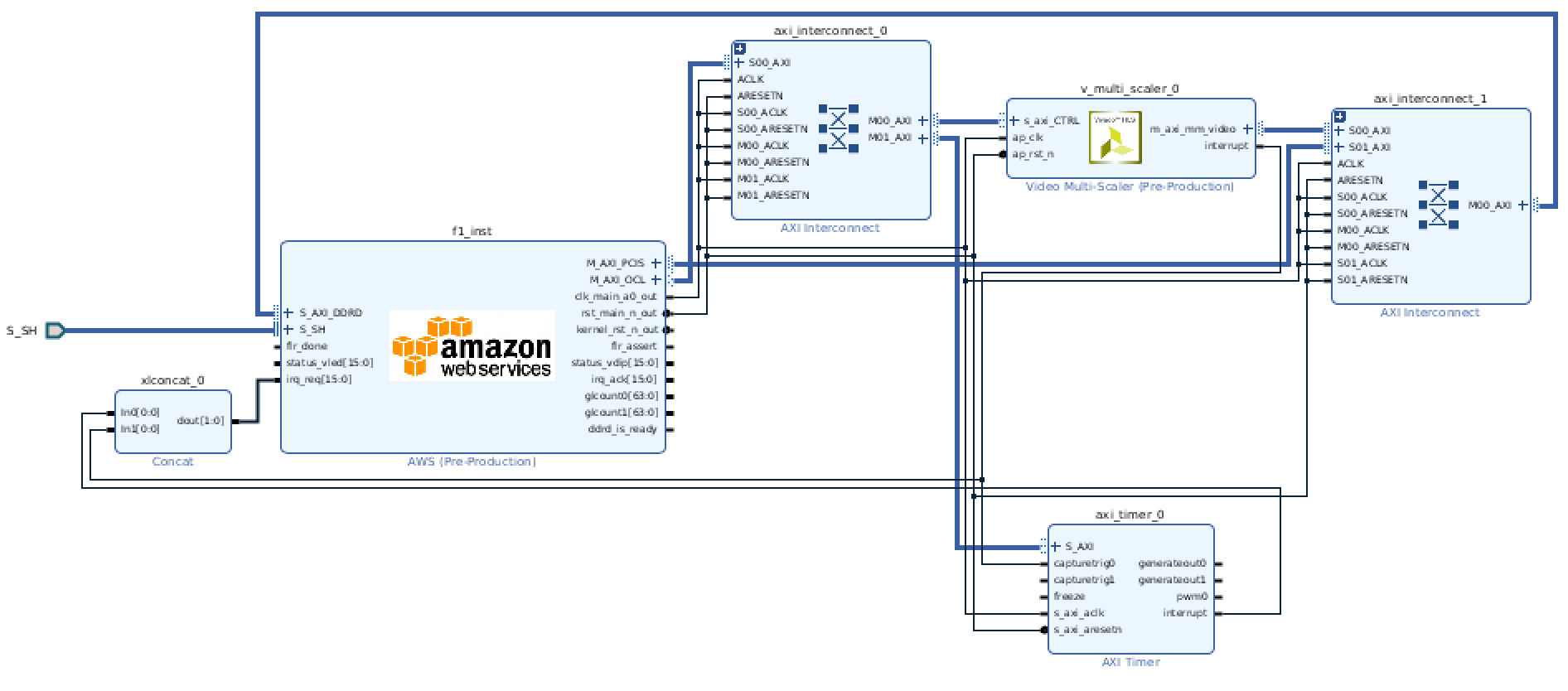
In this diagram:
- All AXI connections go to one of two AXI "interconnects", which are more or less our MMUs (more on this below).
- Via the OCL BAR, we can manipulate the multi-scaler and timer control registers.
- Via the PCIS BAR, we can access the DDR4 memory.
- All clock and reset pins are connected to each other.
- The multi-scaler's video interface is connected to the same AXI interconnect as the DDR4 memory.
- The multi-scaler triggers an interrupt that we can hook into on the host. This can tell us when the current frame is done.
- The multi-scaler also sends its interrupt signal to a "timer". This timer isn't strictly necessary, but can be used by the host to get a cumulative count of completed frames. The timer also gives us an interupt signal should we want to use it.
As mentioned, the AXI interconnect acts as an MMU. This gives us the ability to route each component's reads and writes:
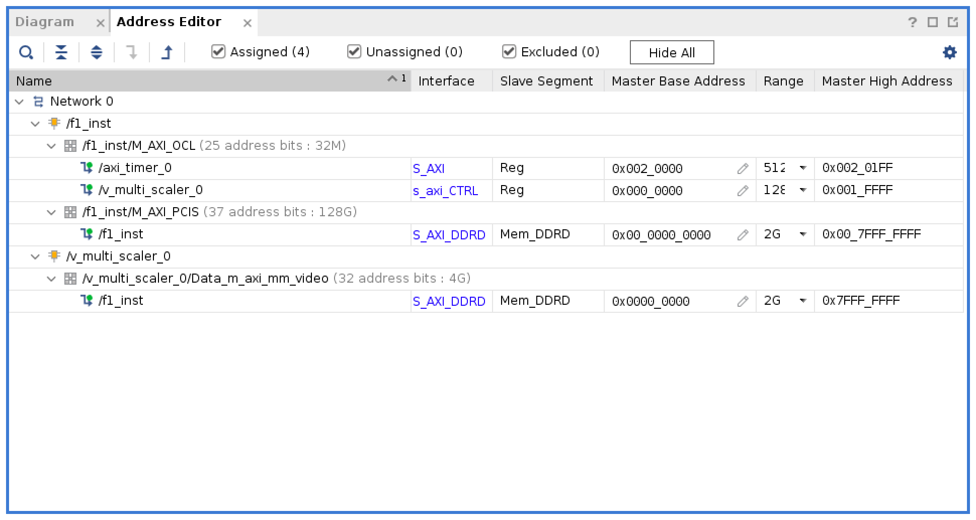
The host is given access to everything, while the multi-scaler only needs DDR4 access. Conveniently we can map most of the addresses to 0, which will simply our code a bit.
Once this design is synthesized and implemented (a process that simply involves waiting for ~2 hours on a c5.9xlarge), you can see the physical layout of your design:
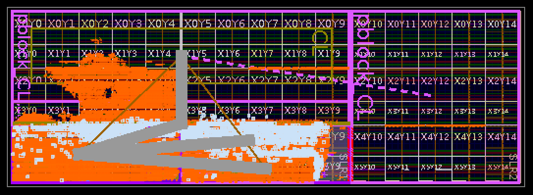
The physical layout is important to ensure that your design can meet its required timing constraints. The F1 FPGA consists of 3 dies stacked on top of each other. Each of these is known as a "super logic region" or "SLR". Crossing SLR boundaries is expensive, so we want to minimize that. For example, we're using the PCIS BAR, which is physically located in the bottom SLR (the left-most in the above image). There are multiple DDR4 channels that we could use, but DDR4 D is used for this design as its physical pins are in the same SLR. Using DDR4 A, which is located in the top SLR, makes it significantly harder to meet timing constraints.
You can upload this design to AWS for conversion into an AFI. Once that's done, the AFI is ready to be loaded onto the F1 instance's FPGA.
The Host Software
Now we'll be making a minimal CLI program to scale a frame. We'll accept a .yuv file as input and output a .yuv file at half the scale. Virtually the entire implementation of this CLI program is going to consist of AXI4 reads and writes via the PCIS BAR.
The AWS HDK provides a C library with the functionality we'll need to do the reads and writes. First, we just need to open handles for the BARs. For example, for the PCIS BAR, which gives us access to the DDR4 memory:
fpga_pci_attach(SLOT_ID, FPGA_APP_PF, APP_PF_BAR4, 0, &g_ddr_bar);Reading/Writing the Frame
The BAR is memory-mapped, so we can just get a pointer that we can read and write like any other memory:
void* get_input_frame_buffer() {
        void* ret = NULL;
        fpga_pci_get_address(g_ddr_bar, 0, MAX_FRAME_BYTES, &ret);
        return ret;
}

const void* get_output_frame_buffer() {
        void* ret = NULL;
        fpga_pci_get_address(g_ddr_bar, MAX_FRAME_BYTES, MAX_FRAME_BYTES, &ret);
        return const_cast<const void*>(ret);
}
Starting the Scaler
First, we need to configure the scaler. We only have to do this once. Once configured, the scaler will stay configured until the FPGA is reset (though in practice, our design would include a mechanism for resetting the scaler without resetting the entire FPGA).
Xilinx provides a library to work with the scaler, but it's simple enough to configure ourselves:
bool configure_scaler() {
        const uint32_t width_in = 7680;
        const uint32_t width_out = 7680 / 2;
        const uint32_t height_in = 4320;
        const uint32_t height_out = 4320 / 2;
        if (false
                || fpga_pci_poke(g_ctrl_bar, 0x4, 1) // global interrupt enable
                || fpga_pci_poke(g_ctrl_bar, 0x8, 3) // interrupt enable (ap_done and ap_ready)
                || fpga_pci_poke(g_ctrl_bar, 0x10, 1) // number of outputs
                || fpga_pci_poke(g_ctrl_bar, 0x100, width_in) // input width
                || fpga_pci_poke(g_ctrl_bar, 0x108, width_out) // output width
                || fpga_pci_poke(g_ctrl_bar, 0x110, height_in) // input height
                || fpga_pci_poke(g_ctrl_bar, 0x118, height_out) // output height
                || fpga_pci_poke(g_ctrl_bar, 0x120, (uint32_t)(((float)height_in * 65536 + height_out / 2) / height_out)) // line rate
                || fpga_pci_poke(g_ctrl_bar, 0x128, (uint32_t)(((float)width_in * 65536 + width_out / 2) / width_out)) // pixel rate
                || fpga_pci_poke(g_ctrl_bar, 0x130, 19) // input format (yuv420)
                || fpga_pci_poke(g_ctrl_bar, 0x138, 19) // output format (yuv420)
                || fpga_pci_poke(g_ctrl_bar, 0x150, width_in) // input stride
                || fpga_pci_poke(g_ctrl_bar, 0x158, width_out) // output stride
                || fpga_pci_poke(g_ctrl_bar, 0x160, 0) // input luma buffer
                || fpga_pci_poke(g_ctrl_bar, 0x170, height_in * width_in) // input chroma buffer
                || fpga_pci_poke(g_ctrl_bar, 0x190, MAX_FRAME_BYTES) // output luma buffer
                || fpga_pci_poke(g_ctrl_bar, 0x200, MAX_FRAME_BYTES + height_out * width_out) // output chroma buffer
        ) {
                return false;
        }

        void* coeffs = NULL;
        if (fpga_pci_get_address(g_ctrl_bar, 0x2000, 0x1000, &coeffs)) {
                return false;
        }
        uint16_t* vertical_coeffs = reinterpret_cast<uint16_t*>(coeffs);
        uint16_t* horizontal_coeffs = reinterpret_cast<uint16_t*>(coeffs) + 0x400;
        for (int phase = 0; phase < 64; phase++) {
                for (int tap = 0; tap < 6; tap++) {
                        horizontal_coeffs[phase * 6 + tap] = k_fixed_coeffs[phase][tap];
                        vertical_coeffs[phase * 6 + tap] = k_fixed_coeffs[phase][tap];
                }
        }

        return true;
}
And once the scaler is configured, we can start it:
bool start_scaler() {
        return !fpga_pci_poke8(g_ctrl_bar, 0, 1);
}
At this point we can wait for the interrupt or just poll the scaler's status until it's done.
The Result
Downscaling an 8K YUV 420 image to 4K YUV 420 appears to take a consistent 66 milliseconds. We actually could have predicted this using the multi-scaler's documentation: We have a 125MHz clock and configured the scaler to process 4 samples per clock cycle: 7680*4320/4/125000000 = 0.066!
That time alone isn't that impressive; You can downscale an 8K frame to 4K in 66 milliseconds without an FPGA. The value of FPGAs for video processing becomes more apparent when you consider:
- We're using a very low clock speed. Doubling this to 250MHz would double the scaling speed.
- This process can be parallelized to the extreme. A single multi-scaler block can scale 8 frames simultaneously. You can add more blocks for even more parallelism.
- The speed is guaranteed. There won't be any jitter in the output. Noisy neighbors won't slow things down. The multi-scaler processes 4 samples per clock cycle, always.
- The multi-scaler uses polyphase scaling as opposed to bilinear or bicubic like you would probably use on a CPU or GPU. In this case, we're using 64-phase, 6-tap polyphase scaling, which isn't very feasible without an FPGA.
All things considered, FPGAs are really good at processing video. For a task as simple as scaling, they're not worth the development cost unless you're already using one, but for more involved tasks (like transcoding), they open up possibilities that simply don't exist elsewhere.
If you're into video processing and you're open to new jobs, Tempus Ex is hiring! Come join us and get paid to work on cool things like what you see here!